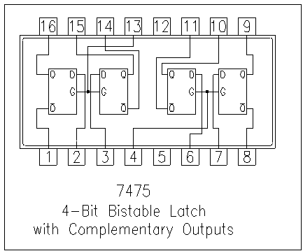
7475 pin diagram
Buy 7475 NS Learn more about 7475 4-BIT BISTABLE LATCHES View the manufacturer and stock and datasheet pdf for the 7475 at Jotrin Electronics. The 7475 contains 4 transparent D latches with a common enable gate on latches 0 and 1 and another common enable on latches 2 and 3.

490 Electronics Ideas In 2022 Circuit Diagram Circuit Diagram
Reviews 0 74HC75 is 4 Bit Bi-Stable Latch 16 Pin IC.
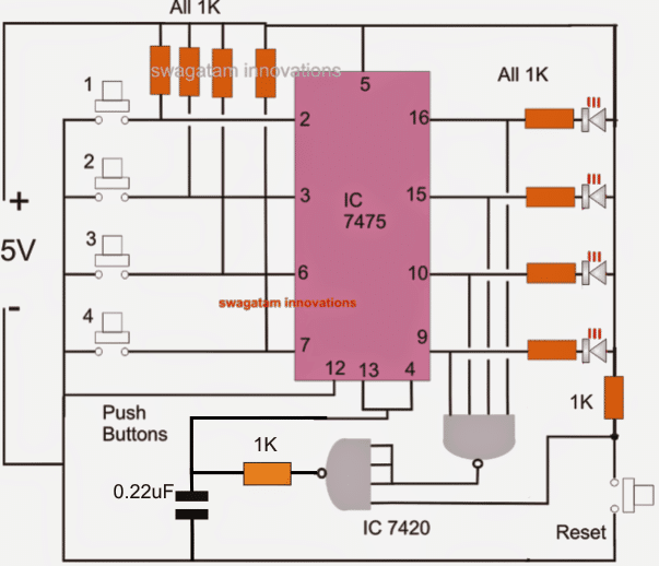
. D flip flop by using IC 7475. Quad D flip flop 7475. All 1R swagatam innovations All 1K 5 ITT 12 16- - 3 IC 7475 15.
IC can operate at -55 to -125 degrees. Connect the CLK to pin 13 on the 7475 chip. This is labeled LE12 or latch enabled input for latches 1 and 2 enabled high.
It contains 4 transparent D latches with common enable gate on latches 0 and 1 and another common enable on latches 2 and 3. Connect the D input to pin 2 on the 7475 chip. Buy 7475 NS Learn more about 7475 4-BIT BISTABLE LATCHES View the manufacturer and stock and datasheet pdf for the 7475 at Jotrin Electronics.
5V swagatam innovations 12 13 4 1K Push. The simulation diagram 7475 i View the full answer Transcribed image text. The given timing diagram shows one positive type of edge triggered d flip flop.
74LS74A Flip Flop Applications It can be used to design a shift. IC 74LS76 draws output voltages for the HIGH state is 35V and for the LOW state is 025V. It contains 4 transparent D latches with common enable gate on latches 0 and 1 and another common enable on latches 2 and 3.
Pin diagram of ic 7475 pin DIAGRAM OF IC 74ls75 logic ic 7475 pin diagram logic diagram of ic 7475 7475 D latch pin diagram of ic 7475 D latch TTL 7475 7475 ic latch Text. D flip flop by using IC 7475. And practical program working process experiment digital electronics machine d latch in hindi video cits nsti Mumbai electronic.
Edge Triggered D flip flop Timing Diagram. The remaining pins are one clock. About Press Copyright Contact us Creators Advertise Developers Terms Privacy Policy Safety How YouTube works Test new features Press Copyright Contact us Creators.
The simulation diagram 7475 i View the full answer Transcribed image text. The simulation diagram 7475 i View. This alloys corrosion resistance and fatigue behavior are.
Edge Triggered D flip flop Timing Diagram.

7475 Lc7475 On Screen Display Controller For Pal Format Video Datasheet 7475 Lc7475 On Screen Display Controller For Pal Format Video Pdf 7475 Lc7475 On Screen Display Controller For

Typical Appearance Of A Friction Spot Weld In En Aw 7475 T761 13 Download Scientific Diagram

Timing Of The 7475 Data Latch Download Scientific Diagram
Aa05llzobqwltm

Flip Flops And Registers Ppt Video Online Download

Ic Pin Diagram Apk Pour Android Telecharger

Electronic Logic
Potenzialverteiler Cbb Tm 04 2x2rc P Pt 2801481 Phoenix Contact
Solved Design Fastest Finger First Indicator Circuit Chegg Com
7475 Datasheet
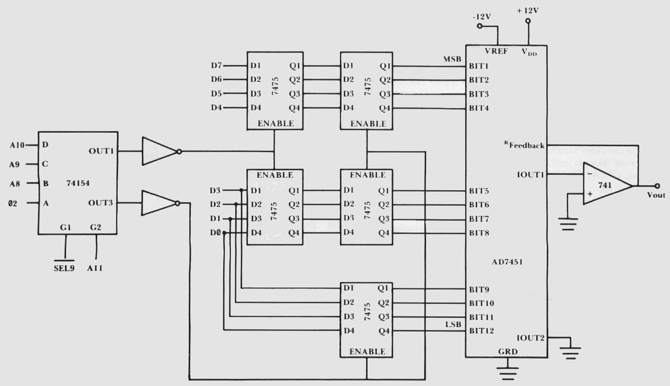
A High Resolution Digital To Analog Converter For The Pet
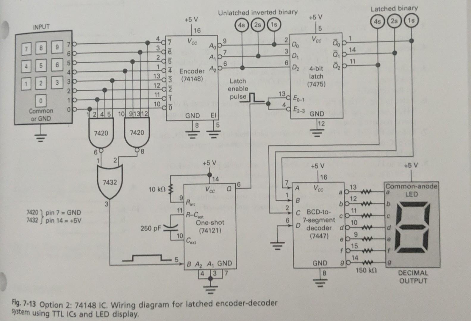
Solved Active Unlatched Inverted Bcd Output Indicators Chegg Com
Skoda Fabia Ii 2009 1 4 Ltr 4hv 63 Kw Engine Identification Characters Bxw As Of May 2008 Wiring Diagrams Pin Connector Location Diagrammata Kalwdiwshs Gia Aytokinhta

Lt8705 Datasheet And Product Info Analog Devices

Ic Pin Diagram Free Download And Software Reviews Cnet Download
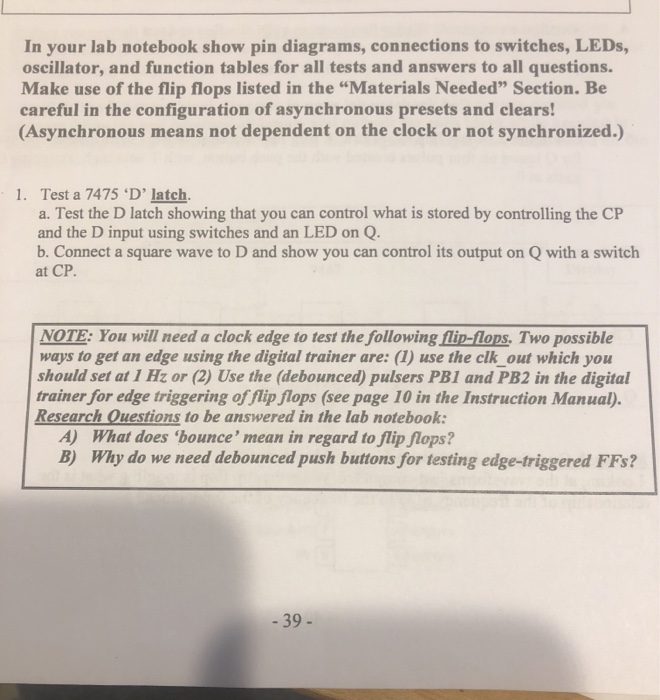
In Your Lab Notebook Show Pin Diagrams Connections Chegg Com

7445 Ic Pinout Diagram Integrated Circuits Elektropage Com